Traditional Moore's Law is dying, and the semiconductor industry knows it. Shrinking transistors on silicon wafers has become brutally expensive and physically punishing. Because brute-force scaling is hitting a wall, chip designers are turning upward instead of inward. They are stacking components in three dimensions.
Enter hybrid bonding. This advanced packaging technique allows silicon dies to connect directly through copper-to-copper bonds, bypassing older micro-bumps that create electrical bottlenecks. It is the hottest battleground in semiconductor manufacturing right now. Global giants and domestic Chinese firms alike are scrambling to own the supply chain for this technology.
The Shift Toward Advanced Packaging
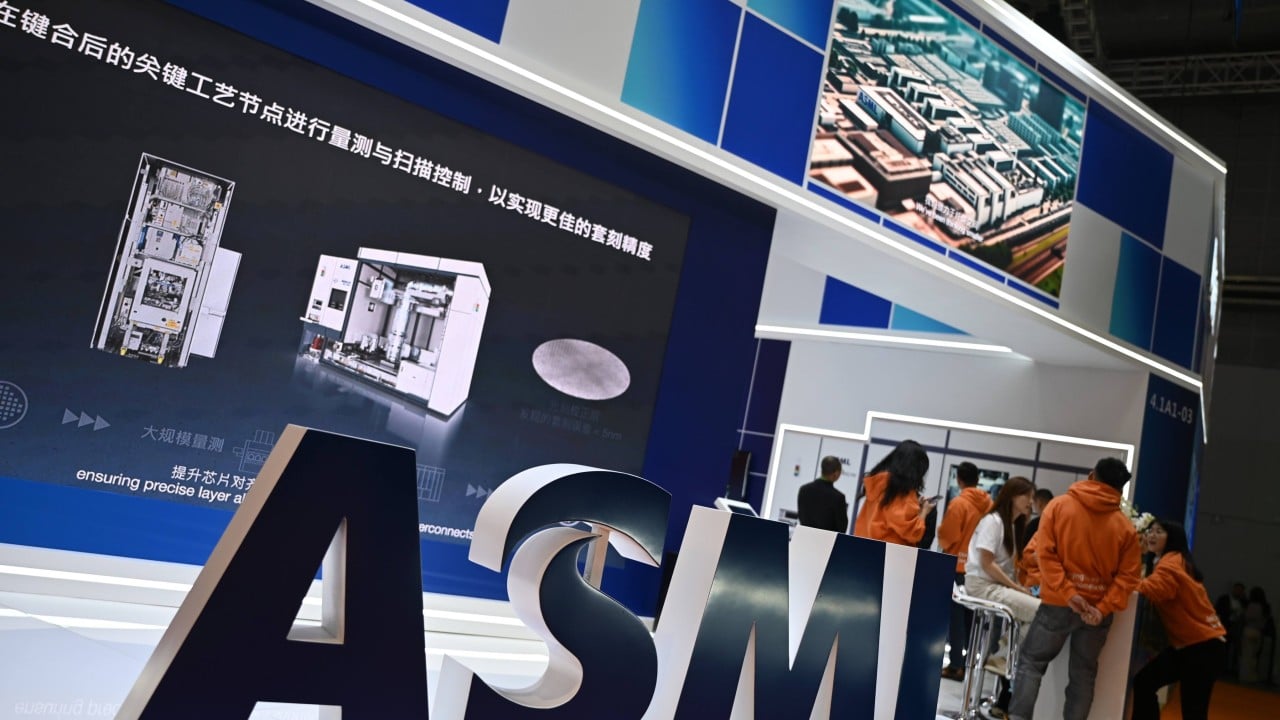
For decades, lithography machines reigned supreme. ASML built an empire on extreme ultraviolet systems that print microscopic circuits onto silicon. But as export curbs tighten and physical limits close in, the industry is shifting focus from front-end lithography to back-end packaging.
Why does packaging matter so much today? Simple physics. When you stack chiplets directly on top of each other using hybrid bonding, electrical signals travel shorter distances. Power consumption drops. Speed increases. It is the primary reason high-performance processors and memory components are breaking performance records. As discussed in detailed reports by Mashable, the effects are notable.
Competitors like Besi have dominated this space with die-to-wafer bonding equipment, but the monopoly is cracking. Industry reports reveal that ASML is actively developing its own track-based hybrid bonding tool design, partnering with firms like Prodrive Technologies and VDL ETG. Patents filed between late 2022 and 2024 show the Dutch lithography titan laying groundwork for a massive expansion into back-end processes.
Inside ASML's Track-Based Approach
Conventional bonding machines use a bond head that picks up an individual die from a diced wafer and places it onto a target site. ASML’s emerging design throws out that playbook.
Instead of a traditional pick-and-place arm, ASML's conceptual architecture moves each die on its own individual holder around a dedicated track. The die travels past distinct inspection, cleaning, plasma activation, and measurement stations before arriving at a final bonding station. At that point, a precision chuck lifts the bottom wafer upward to meet the prepared die.
This track-based layout targets the two biggest killers of manufacturing yield: particle contamination and micro-misalignment. By handling dies individually through a controlled loop, the system aims to solve the precision issues that have kept die-to-wafer hybrid bonding limited mostly to high-end logic chips, such as AMD's V-Cache architecture.
Building such a system is no small feat. Engineering hurdles remain massive. Feed-forward metrology, reliable die-to-wafer contact, and maintaining an ultra-clean processing loop are severe roadblocks. Analysts expect ASML to price its eventual hardware at a steep premium, targeting top-tier fabs that demand absolute perfection.
The Domestic Push in China
While Western equipment makers duel over future tool designs, Chinese semiconductor firms are adapting out of necessity. Facing strict export controls on advanced extreme ultraviolet and deep ultraviolet lithography gear, domestic players are leaning heavily into advanced packaging to extract more performance from mature silicon nodes.
Domestic equipment suppliers are pouring capital into research and development to close the technological gap. Companies like Piotech have reported surging revenues from thin-film deposition tools and hybrid bonding equipment lines. Meanwhile, architectures pushed by tech giants like Huawei are driving massive domestic demand for packaging and deposition hardware.
Rather than waiting for foreign tool imports that may never arrive, local supply chains are building a parallel ecosystem. They are betting that clever packaging can offset the inability to print sub-2-nanometer transistors using restricted lithography.
What Comes Next for Semiconductor Manufacturing
Hybrid bonding is no longer just an experimental laboratory trick. It is scaling up in production lines worldwide, transforming how microchips are assembled.
For ASML, moving into packaging represents a logical evolution. It protects their market dominance as pure lithography growth slows down. For Chinese chipmakers, mastering these packaging techniques is an existential requirement to stay competitive on the global stage.
The race is on, and the winner won't just control how circuits are printed. They will control how entire systems are built from the silicon up.


